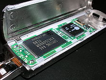
Flash Memory
90 nm technology
Website
Date Added
1 January 2007
Company
Country of Origin
Categories
Subcategories
"Samsung is the industry's first manufacturer to apply 90-nanometer process technology to a Flash memory device, ushering in the era of ultra-high-capacity non-volatile memory technology. The 2Gb device's cutting-edge, 0.05 μm2 design rule is half the minimum cell size found in other NAND Flash memory chips. The ultra high capacity device can make for an affordable 256 MByte USB Flash drive, expediting the replacement of the floppy drive and zip drive combination." "Samsung's new NAND Flash memory device has been designed for production on the company's existing fabrication lines, eliminating the need for additional facilities investments. The utilization 90-nanometer process technology greatly reduces manufacturing cost, enabling Samsung to produce the world's highest capacity 2Gb NAND Flash memory device while remaining the industry's competitive price leader." "Samsung's 2Gbit Flash memory utilizes a novel SSA-STi (Sacrificial Self Align Shallow Trench isolation) for the isolation technology developed to improve cell data storage reliability, which was considered most challenging at sub-100nm process. This technology breakthrough has enabled Samsung to develop the 2Gb NAND Flash memory device a year earlier than planned."
Supporting Info URL
"This review compares ten basic USB flash drives that can easily create a portable solution for your data and media. They are small yet can supply up to 64GB of memory. We compared the most popular memory sizes of 8GB, 16GB and 32GB. The 32GB USB drives can store up to 14,970 5-megapixel images or 4390 minutes of MPEG4 video." 'A good USB flash drive can greatly increase your productivity and flexibility. Some are even fast enough to stream video so you can easily view your entertainment on a variety of your devices. The larger versions can even store enough video, data and images to act as your backup solution. This review compares the best of the basic, no-fuss USB drives that are dependable, fast and well supported.'
"Intel's 90 nm flash technology delivers industry leading 0.076 μm2 flash single bit memory cell at 210 nm pitch which translates to 0.038 μm2 bit size with multi-level-cell (MLC), using 193 nm lithography and Cu interconnect [Y. Song (2003)]. The 193 nm lithography required significant etch improvement especially at flash gate patterning with multi-layer gate stack and contact patterning due to reduced etch selectivity to resist. The other technology enablers are advanced STI gap fill, improved process at self-aligned-polysilicon (SAP) polish to enable vertical scaling, improved oxidation for trench sidewall oxidation, advanced cleaning tool to reduce defects for data retention and cycling endurance, and improved contact patterning and dielectric strength film to endure the program/erase cycles at reduced contact to gate spaces." Pangai, K; Abraham, C.; Wang, M.; Hien Nguyen; Coulter, J; Begley, T.; Soss, S. (2005)
"A 1.8-V 2-Gb NAND flash memory has been successfully developed on a 90-nm CMOS STI process technology, resulting in a 141-mm2 die size and a 0.044-μm2 effective cell. For the higher level integration, critical layers are patterned with KrF photolithography. The device has three notable differences from previous generations. 1) The cells are organized in a single (16K+512) column and 128K row array by adopting a one-sided row decoder in order to minimize the die size. 2) The bitline precharge level is set to 0.9 V in order to increase on-cell current. 3) During the program operations, the string select line, which connects the NAND cell strings to the bitlines, is biased with sub-VCC in order to avoid program disturbance issues." Lee, J.; Sung-Soo Lee; Oh-Suk Kwon; Kyeong-Han Lee; Yong-Ho Lim; Byung-Soon Choi; Jong-Sil Lee; Wang-Chul Shin; Jeoing-Hyuk Choi; Kang-Deog Suh (2003)
Nanomaterials
Shape/Dimensions
90 nm
Shape/Dimensions (source)
Functions of Nanomaterial
Location of Nanomaterial
Potential Exposure Pathways
How much we know
Additional Information